International Journal of Optics and Photonic Engineering
(ISSN: 2631-5092)
Volume 4, Issue 2
Research Article
DOI: 10.35840/2631-5092/4519

Article Formats
Tuning the Oxygen Content in the Nb2O5 Thin Films Deposited on Si by DC Magnetron Sputtering for Energy Storage Devices Applications
Table of Content
Figures
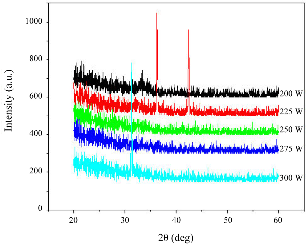
Figure 1: XRD pattern of Nb2O5 deposited on silicon...
XRD pattern of Nb2O5 deposited on silicon substrate by magnetron sputtering at selected deposition powers.
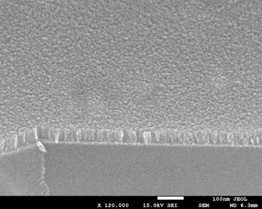
Figure 2: An inclined view (50.1o) of a 300W-deposited...
An inclined view (50.1°) of a 300W-deposited Nb2O5 thin film.
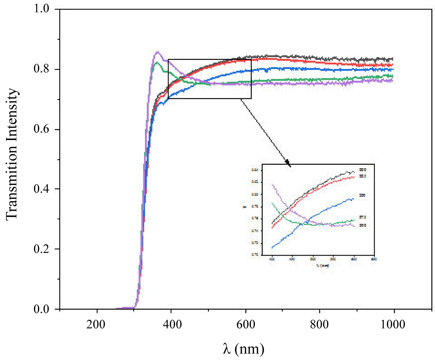
Figure 3: Transmission intensity of Nb2O5 thin films...
Transmission intensity of Nb2O5 thin films deposited on glass substrates.
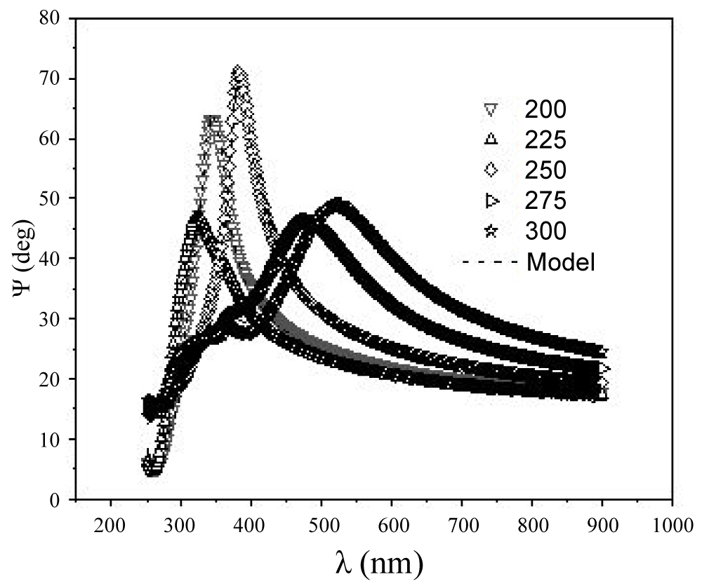
Figure 4: Ellipsometry parameter Ψ measured for the...
Ellipsometry parameter Ψ measured for the Nb2O5 thin films deposited at the powers 200 W up to 300 W, dotted lines correspond to the fitting model.

Figure 5: Ellipsometry parameter ∆ measured for the Nb2O5...
Ellipsometry parameter ∆ measured for the Nb2O5 thin films deposited at the powers 200 W up to 300 W, dotted lines correspond to the fitting model.

Figure 6: Refractive index of Nb2O5 thin films deposited...
Refractive index of Nb2O5 thin films deposited on a silicon substrate.

Figure 7: Nb2O5 energy band gap determination due...
Nb2O5 energy band gap determination due to direct transition.
Tables
Table 1: 225 W Nb2O5 thin film lattice parameters and grain size extracted from XRD pattern.
Table 2: Percentage ratios of the Nb atoms to O contents of the Nb oxides deposited on a silicon substrate at different deposition powers.
Table 3: Nb2O5 thin films thicknesses extracted from ellipsometry data.
References
- M Ieong, Doris B, Kedzierski J, Rim K, Yang M (2004) Silicon device scaling to the sub-10-nmr. Science 306: 2057-2060.
- ML Green, EP Gusev, R Degraeve, EL Garfunkel (2001) Ultrathin (< 4 nm) SiO2 and Si-O-N gate dielectric layers for silicon microelectronics: Understanding the processing, structure, and physical and electrical limits. J Appl Phys 90: 2057-2121.
- J Robertson (2000) Band offsets of wide-band-gap oxides and implications for future electronic devices. J Vac Sci Technol B Microelectron Nanom Struct 18: 1785.
- GD Wilk, RM Wallace, JM Anthony (2001) High-κ gate dielectrics: Current status and materials properties considerations. J Appl Phys 89: 5243-5275.
- KT Jacob, C Shekhar, M Vinay, Y Waseda (2010) Thermodynamic properties of niobium oxides. J Chem Eng Data 55: 4854-4863.
- DM Alsebaie, W Shirbeeny, A Alshahrie, MS Abdel-Wahab (2017) Ellipsometric study of optical properties of Sm-doped ZnO thin films Co-deposited by RF-Magnetron sputtering. Optik 148: 172-180.
- HA Al-Khanbashi, W Shirbeeny, AA Al-Ghamdi, LM Bronstein, WE Mahmoud (2014) Spectroscopic ellipsometry of Zn1-xCuxO thin films based on a modified sol-gel dip-coating technique. Spectrochim Acta - Part A Mol Biomol Spectrosc 118: 800-805.
- W Shirbeeny, F Talbi (2017) Improved photon trapping by combined use of dye-synthesized and one-dimensional fiber-like nanostructured CuO thin film. Optik 147: 14-21.
- A Chelouche, T Touam, M Tazerout, D Djouadi, F Boudjouan (2017) Effect of Li codoping on highly oriented sol-gel Ce-doped ZnO thin films properties. J Lumin 188: 331-336.
- GEJJ, FA Modine (1996) Parameterization of the optical functions of amorphous materials in the interband region. Appl Phys Lett 69: 371.
- U Pal, D Samanta, S Ghorai, AK Chaudhuri (1993) Optical constants of vacuum‐evaporated polycrystalline cadmium selenide thin films. J Appl Phys 74: 6368-6374.
Author Details
Waleed Elshirbeeny, PhD.1,2*, Mohannad A Harthy, MSc.1, and Ahmed A Alshahrie, PhD.1
1Department of Physics, Faculty of Sciences, King Abdulaziz University, Saudi Arabia
2Department of Physics, Faculty of Science, Alexandria University, Egypt
Corresponding author
Waleed Elshirbeeny, Department of Physics, Faculty of Sciences, King Abdulaziz University, Saudi Arabia; Department of Physics, Faculty of Science, Alexandria University, Egypt
Accepted: October 12, 2019 | Published Online: October 14, 2019
Citation: Elshirbeeny W, Harthy MA, Alshahrie AA (2019) Tuning the Oxygen Content in the Nb2O5 Thin Films Deposited on Si by DC Magnetron Sputtering for Energy Storage Devices Applications. Int J Opt Photonic Eng 4:019
Copyright: © 2019 Elshirbeeny W, et al. This is an open-access article distributed under the terms of the Creative Commons Attribution License, which permits unrestricted use, distribution, and reproduction in any medium, provided the original author and source are credited.
Abstract
Nb2O5 thin films were deposited on silicon substrate using DC magnetron sputtering by applying variable deposition power on a Nb target and fixing the oxygen flow rate during the deposition process. This technique helped the control of thin film thickness and oxygen-to-metal ratio. Successive deposition powers between 200 W up to 300 W were applied. The minimum thin film thickness was about 25 nm, and the corresponding energy band gap was 3.59 eV. The thin films showed high transmittance and refractive index in the visible region. These characteristics match the high-k materials requirements as replacement of SiO2 layer in energy storage devices and DRAM applications.
Keywords
High-K materials, Energy storage devices, Metal oxides
Introduction
The complementary metal oxide semiconductor silicon-based field effect transistor has been the most important electronic device for about 40 years. Its stability and low power consumption encouraged engineers to increase the number of CMOS SiO2-based FET in microprocessors and integrated circuits. However, the need for the thin-sized memory storage devices forced the reduction of the SiO2 layer size. Accordingly, the SiO2 layer used as a gate had its size reduced down to about 1.2 nm. At this size, direct tunneling of electrons becomes inadequately very high, which lead to undesirable power dissipation [1,2]. It is also challenging to deposit such unreliable thin film. The solution to such problem of tunneling current is to replace the SiO2 thin film with a thicker layer of a high-k material, or (high-k metal oxide). The main essential requirement for the replacement metal oxide is that the k value should be more than 12 and the metal oxide should have a wide energy bandgap. Though, it has been noticed that the k value behaves inversely with the energy bandgap of the metal oxide [3]. The requirements of the replacement high-k metal oxides should be stated herein; the oxide should be thermodynamically stable, and in order to minimize carrier injection into metal oxide band it should have band offset with silicon over 1 eV. Additionally, it must have fewer electrically-active defects [3,4]. There are various oxides of considerable k-value but with a relatively small energy bandgap, such as Ta2O5, Nb2O5 and SrTiO3. Among them Nb2O5 has the most chemical stability. It is considered as good optical material as it has good resistance to corrosion in any media, it is thermodynamically stable to be formed [5], it has a high refractive index in the UV-VIS region and of high transparency with a relatively wide energy bandgap. Since it is a transparent dielectric material, Nb2O5 is ideal for super capacitor technology applications such as energy storage devices and DRAM modules.
In this paper, we focused on developing Nb2O5 thin films of variable metal-to-oxygen content by employing sputtering technique with constant Argon-to-Oxygen ratio but applying different deposition powers on the Nb target. Successive Nb2O5 thin films were deposited on Si and glass substrates by applying deposition powers in the range of 200 W up to 300 W, step 50 W. The energy band gap, crystal structure, surface morphology, and metal - to- oxygen content, were studied VS deposition power. Refractive index, extinction coefficient, transmittance, Eg, thin film thicknesses, and roughness were also determined using Variable Angle Spectroscopic Ellipsometry (VASE) which has been a successful technique that helped exact determination of such optical parameters [6,7].
Experimental
Synthesis of Nb2O5 thin films
Nb target of diameter 3", thickness 0.6", and purity 99.99%, was used in DC magnetron sputtering operated at the 200 up to 300 W, step 50 W. Nb target was obtained from China Rare Material Co. Ltd. The vacuum pressure was initiated at 8.4 × 10⁻⁶ mbar. Argon and oxygen mixture by Ar-to-O ratio 95:5 was used as an inert gas and oxidation agent, respectively. The flow rate was adjusted and fixed at 90 sccm. The silicon (111) and glass substrates of thickness 2 mm were held at 10 cm from the Nb target. SiO2 layer was removed using plasma pre-deposition for 30 seconds. Working pressure reached 4.8 × 10⁻² mbar during the deposition process. The deposition time was adjusted at 60 minutes in each run. The substrate holder was kept rotating at a fixed rate.
Characterization
The crystal structure of Nb2O5 thin films was investigated using high-resolution X-ray diffractometer (Ultima-IV; Rigaku, Japan) with Cu Kα line of wavelength 0.15406 nm operated at 40 kV and 20 mA. The surface morphology, roughness, and thickness were examined using (FESEM-JSM-7600F; JEOL, Japan). Thin film elemental composition was studied using energy-dispersive x-ray spectroscopy (EDX). VASE parameters, Ψ and Δ, were measured for the thin films using M-2000 Variable Angle Spectroscopic Ellipsometer (J. A. Woollam Co., Inc.).
Results and Discussion
XRD characterization of Nb2O5 thin films
Figure 1, shows the XRD pattern of the Nb2O5 thin films deposited at powers 200 W up to 300 W with step 50 W. The 225 W Nb2O5 thin film showed considerable diffraction peaks at 2θ = 36.24, and 42.46°. According to XRD card number PDF #721484, the corresponding atomic planes are (541) and (811), respectively. This data indicates a tetragonal crystal structure. The 300 W Nb2O5 thin film showed a sharp peak at the 2θ = 31.26°. All other thin films exhibited an amorphous structure. Such variation in crystal structure indicated the influence of the oxygen content variation with deposition power applied to Nb target. The interplanar spacing dhkl is conveniently written in terms of diffraction angle θ as follows [8]
The grain size D was calculated using the Scherrer's formula [9]
where β is the full width at half maximum of the diffraction peak.
The lattice constants a and c were estimated using the tetragonal crystal identity
The lattice constants, the grain size and the lattice parameters h, k, and l, are listed in Table 1 (Figure 1).
FESEM morphology of Nb2O5 thin films
The morphology, thickness, and deposited particles shape were examined using FESEM. Figure 2 provides valuable information about the surface roughness, the thickness, the grain shape and size, the uniformity and homogeneity of the 300 W Nb2O5 thin film, taken as an example. The Φ = 50.1o inclined view and the scale on the picture indicates a thin film thickness (t) of about 72 nm, calculated as follows
Where tinclined is the thickness of the inclined view, which is in this case is 46.6 nm and t is the calculated thickness which is 72.6 nm. It is noticed in Figure 2 that the thin film is uniformly distributed on the substrate and the thin film composition is homogeneous (Figure 2).
EDX analysis
The atomic percentage of Nb to O in Nb2O5 thin films deposited at the indicated powers are listed in Table 2. The variation in the weight ratios provides valuable information about the effect of deposition power on the oxygen-to-metal content (Table 2).
Optical characterization
Transmission intensity for all thin films was measured by aligning the VASE ellipsometer at 0o angle of incidence on the thin film deposited on a glass substrate. The thin films showed transmission intensity of about 0.85 at the visible region of the spectrum. Sharp absorption occurred at about 350 nm, which approximately corresponds to an energy gap of about 3.54 eV. The inset graph on Figure 3 shows the variation of the transmission intensities for thin films deposited at the indicated powers (Figure 3).
Nb2O5 thin films deposited on silicon were considered as composed of a system of three layers, Si substrate, SiO layer of thickness 3 nm and Nb2O5. The measured spectrum of the ellipsometry parameters Ψ and Δ was then fitted to a Tauc-Lorentz oscillator model [10] which is a successful fitting model in case of amorphous materials,
for E > Eg
Where A, Eo, Er, and Eg are the oscillator amplitude, the peak energy, the peak broadening, and the energy band gap, respectively. ε2(E) is the imaginary part of the refractive index which is a function of photon energy. Ψ and Δ were measured at different angles of incidence; though, we selected the proper angle of incidence which corresponds to a maximum change of the plane of polarization and abrupt phase change. The fitted ellipsometry parameters are shown in Figure 4 and Figure 5.
The refractive index VS. incident photon wavelength shown in Figure 6 was extracted after fitting Ψ and Δ. Fitting ellipsometry parameters revealed the extinction coefficient K and the thin film thicknesses, which were confirmed by FESEM results. Tauc-Lorentz model was successfully employed not only in the visible region but also covered the UV region 200-400 nm as well. The direct band gap in the Nb2O5 was calculated using the extracted extinction coefficient and refractive index according to the relation [11],
α is the absorption coefficient calculated using the relation , where K is the extinction coefficient. Here, n equals to 1/2 in case of direct energy gap semiconductor. The relation between VS. is shown in Figure 7. Eg values and the thickness of the thin films deposited at the powers 200W up to 300W are listed in Table 3 (Figure 6 and Figure 7).
Conclusion
Thin films of Nb2O5 were successfully grown on silicon and glass substrates using DC magnetron sputtering using new technique by applying variable deposition power on a Nb target while keeping the oxygen flow constant. XRD verified that the crystal structure varied according to the deposition power. EDX revealed an alternative Nb-to-O ratio against deposition power. FESEM proved uniform thickness and homogeneous Nb2O5 distribution on the substrate surface. By employing this technique, it is possible to tailor the energy gap of Nb2O5 with thickness down to about 25 nm which has a potential application in energy storage devices and SiO2 replacement in CMOS integrated circuits.