International Journal of Nanoparticles and Nanotechnology
(ISSN: 2631-5084)
Volume 3, Issue 1
Research Article
DOI: 10.35840/2631-5084/5513

Article Formats
Tuning Electrical and Optical Properties of Transparent Conductive Thin Films Using ITO and ZnO Nanoparticles, Sol-Gel-ZnO and Ag Nanowires
Table of Content
Figures
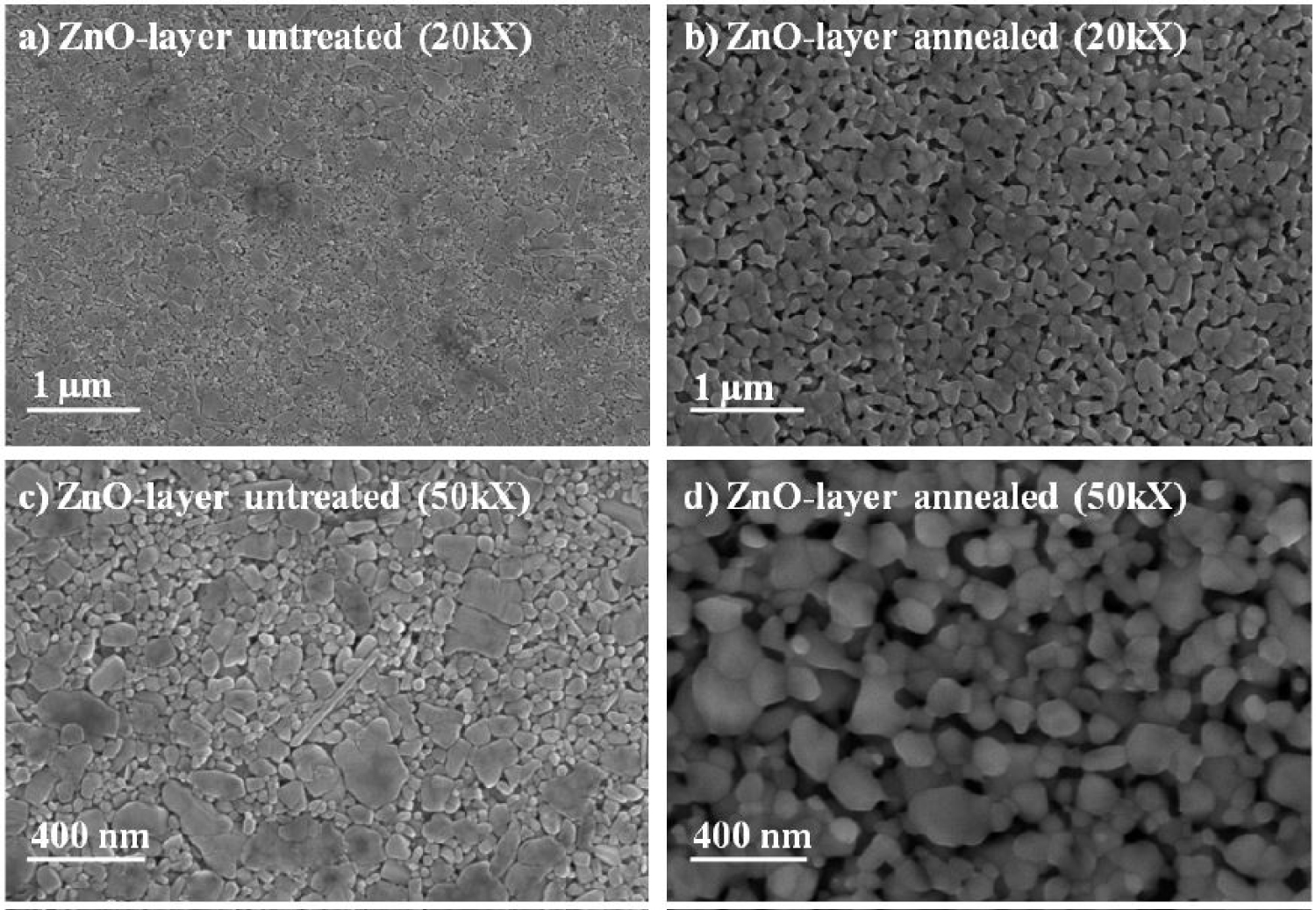
Figure 1: SEM top view of as deposited and annealed ZnO...
SEM top view of as deposited and annealed ZnO nanoparticle films. The annealing at 800 ℃ sinters the particles together, while also reducing the layer thickness from 630 nm to 560 nm.
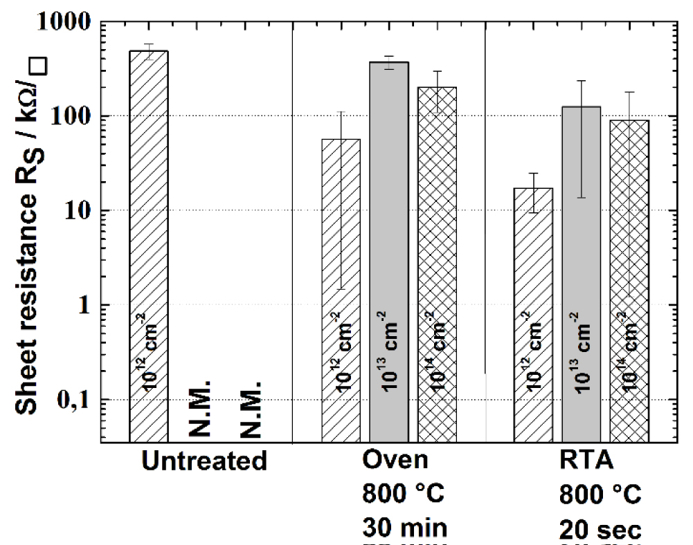
Figure 2: Sheet resistance for different post-ion-implantation-annealing...
Sheet resistance for different post-ion-implantation-annealing. Untreated samples of 1013 and 1014 cm-2 were not measurable. Tube furnace annealing and Rapid Thermal Annealing (RTA) reduce sheet resistance significantly. The best result is achieved with 1012 cm-2 dose and RTA.

Figure 3: SEM top view of ion implanted ZnO nanoparticle...
SEM top view of ion implanted ZnO nanoparticle films after implantation with different doses, after RTA and after annealing in furnace. Higher doses radiation damage breaks sintering necks between grains which is only slightly repaired by annealing.
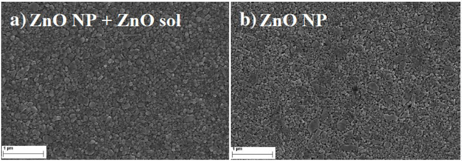
Figure 4: SEM top view of ZnO nanoparticle films...
SEM top view of ZnO nanoparticle films before and after infiltration with doped ZnO-sol. Wetting of ZnO particles with the sol enhances contact area and sintering neck formation as well as filling the empty spaces between particles.
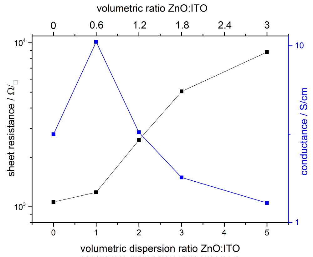
Figure 5: Sheet resistance and conductance for different mixtures...
Sheet resistance and conductance for different mixtures of ZnO and ITO nanoparticles. The best result is achieved with a volumetric ratio of ZnO:ITO of 0.6.
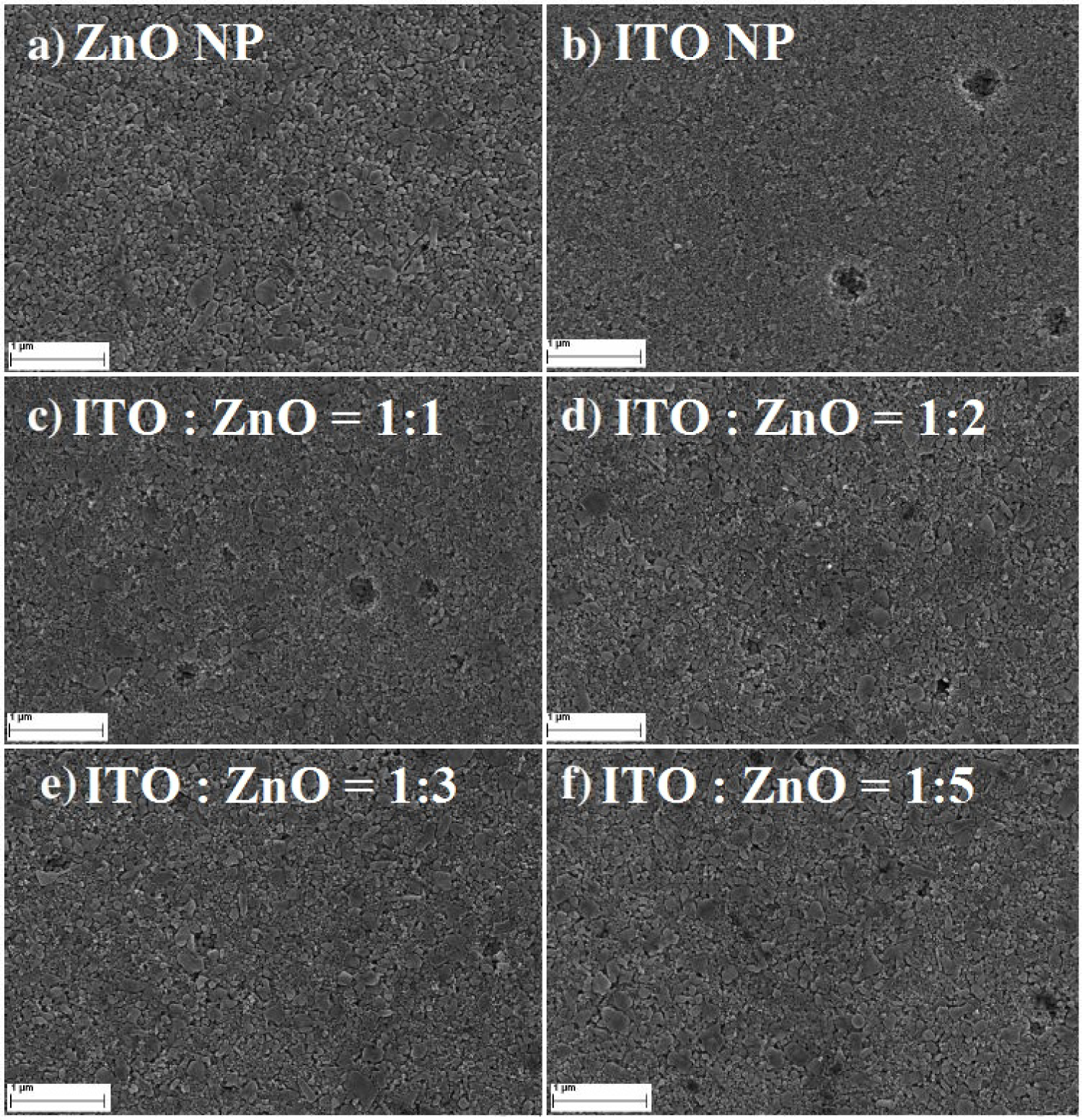
Figure 6: SEM top view of different mixtures of...
SEM top view of different mixtures of ZnO and ITO nanoparticles shows good intermixing with no tendencies of separation. The higher the ZnO amount the more the morphology resembles the pure ZnO morphology with broader particle size distribution than pure ITO. Moreover, mixed films seem more densely packed than pure ZnO films.
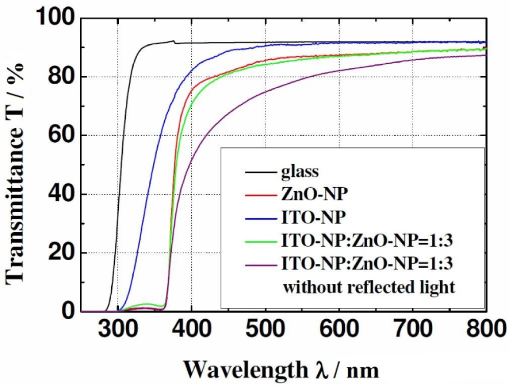
Figure 7: Wavelength dependent change in transmittance for pure...
Wavelength dependent change in transmittance for pure ZnO, ITO as well as a mixture. All mixtures resemble the behavior of pure ZnO films independently of mixing ratio, thus only one exemplary spectrum is shown.
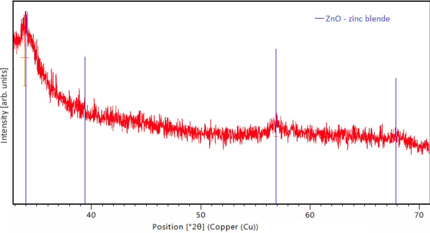
Figure 8: XRD spectrum of an as-deposited sol-gel ZnO...
XRD spectrum of an as-deposited sol-gel ZnO thin film after drying at 230 ℃. Zinc blende structure ZnO can be identified and no by-products are present.
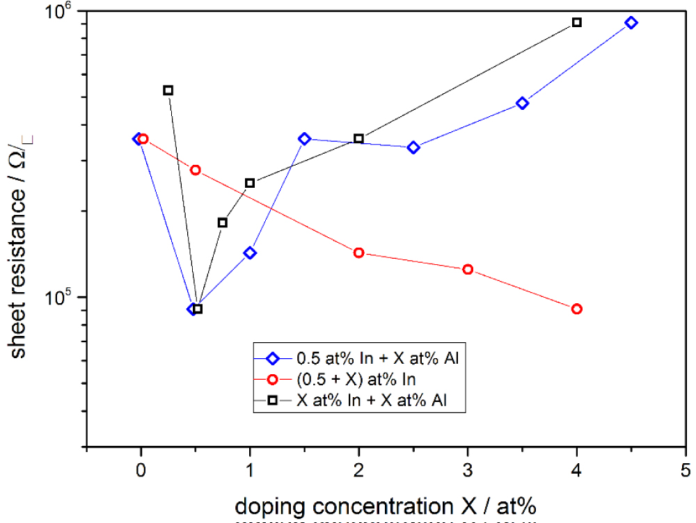
Figure 9: Sheet resistance of ZnO sol-gel films...
Sheet resistance of ZnO sol-gel films for different doping concentrations. The red circle shows a purely In-doped sol, the blue diamond represents a sol fixed at 0.5 at% In and variation of Al content, and the black square stands for an equal doping of In and Al.
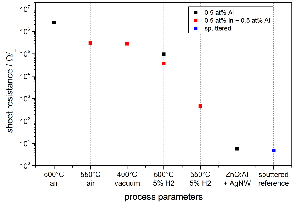
Figure 10: Sheet resistance of ZnO sol-gel films with different annealing...
Sheet resistance of ZnO sol-gel films with different annealing parameters. The temperature was varied from 400-550 ℃ and the atmosphere changed from air to vacuum to 5% H2 in N2 forming gas. Finally, the sample with Ag-NW and a 1 µm sputtered reference are added to the figure as a comparison.
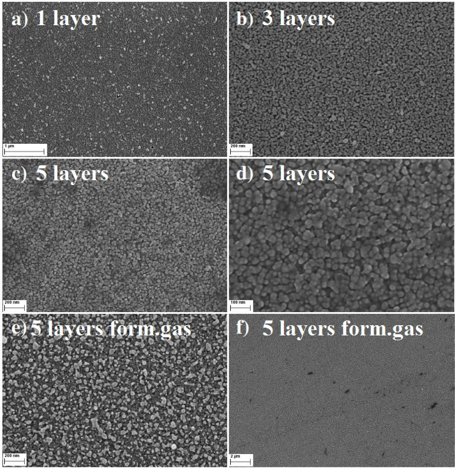
Figure 11: SEM top view of ZnO films with multiple coatings annealed...
SEM top view of ZnO films with multiple coatings annealed in air or 5% H2 in N2 forming gas at 550 ℃. Repeated sol coating infiltrates previously formed crystals, enhancing sintering behavior and lowering porosity. The atmosphere does not seem to have huge influence on morphology.
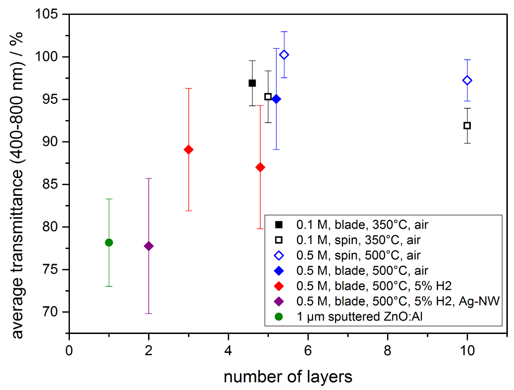
Figure 12: Average transmittance of different sol-gel derived ZnO:Al,...
Average transmittance of different sol-gel derived ZnO:Al,In films. Deposition methods were spin coating and doctor-blading, the annealing was performed in air and under 5% H2 in N2 forming gas. Finally, the sample with Ag-NW is shown as well as a 1 µm sputtered reference as a comparison.
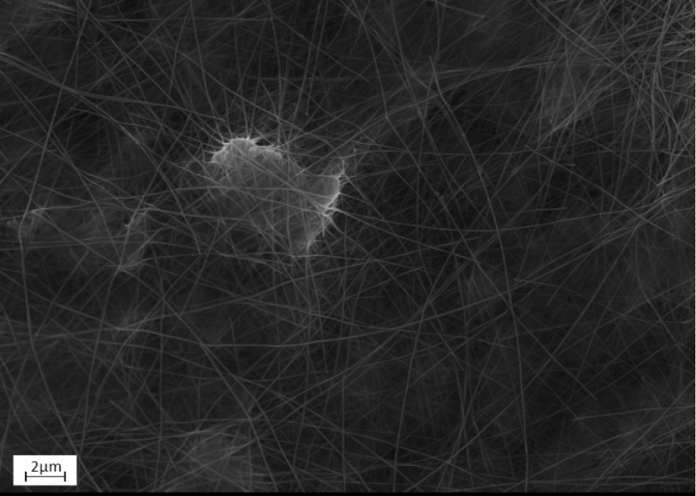
Figure 13: Percolation network of silver...
Percolation network of silver nanowires (Ag-NW) on top of sol-gel derived ZnO:Al film.
References
- T Schuler, MA Aegerter (1999) Optical, electrical and structural properties of sol gel ZnO:Al coatings. Thin Solid Films 351: 125-131.
- T Minami (2005) Transparent conducting oxide semiconductors for transparent electrodes. Semiconductor Science and Technology 20: 35-44.
- H Oh, J Krantz, I Litzov, T Stubhan, L Pinna, et al. (2011) Comparison of various sol-gel derived metal oxide layers for inverted organic solar cells. Solar Energy Materials and Solar Cells 95: 2194-2199.
- M Miyake, H Fukui, T Hirato (2012) Preparation of Al-doped ZnO films by aqueous solution process using a continuous circulation reactor. Physica Status Solidi 209: 945-948.
- H Hagendorfer, K Lienau, S Nishiwaki, CM Fella, L Kranz, et al. (2014) Highly transparent and conductive ZnO: Al thin films from a low temperature aqueous solution approach. Adv Mater 26: 632-636.
- P Fuchs, H Hagendorfer, YE Romanyuk, AN Tiwari (2015) Doping strategies for highly conductive Al-doped ZnO films grown from aqueous solution. Physica Status Solidi 212: 51-55.
- T Kuwabara, X Wang, T Kusumi, T Yamaguchi, T Taima, et al. (2016) Flexible inverted polymer solar cells fabricated in air at low temperatures aqueous solution. Japanese Journal of Applied Physics 55.
- YQ Liu, DD Zhang, HX Wei, QD Ou, YQ Li, et al. (2017) Highly efficient quantum-dot light emitting diodes with sol-gel ZnO electron contact. Optical Materials Express 7: 2161-2167.
- J Krantz, M Richter, S Spallek, E Spiecker, CJ Brabec (2011) Solution-Processed Metallic Nanowire Electrodes as Indium Tin Oxide Replacement for Thin-Film Solar Cells. Advanced Functional Materials 21: 4784-4787.
- T Stubhan, J Krantz, N Li, F Guo, I Litzov, et al. (2012) High fill factor polymer solar cells comprising a transparent, low temperature solution processed doped metal oxide/metal nanowire composite electrode. Solar Energy Materials and Solar Cells 107: 248-251.
- B Wei, S Pan, T Wang, Z Tian, G Chen (2016) Solution-processed Ag-nanowire/ZnO- nanoparticle composite transparent electrode for flexible organic solar cells. Nanotechnology 27: 505208.
- ZZ You, GJ Hua, YC Yong, H Jin (2012) Microstructural and optoelectrical properties of transparent conducting ZnO:Al thin films for organic solar cells. Crystal Research & Technology 47: 1039-1046.
Author Details
M Schuster*, S Groß, F Roider, I Maksimenko and PJ Wellmann
Department of Materials Science 6, Materials for Electronics and Energy Technology, Friedrich-Alexander-University Erlangen-Nürnberg, Germany
Corresponding author
Matthias Schuster, Department of Materials Science 6, Materials for Electronics and Energy Technology, Friedrich-Alexander-University Erlangen-Nurnberg, Martensstr 7, 91058 Erlangen, Germany, Tel: +49-(0)-9131/85-27719, Fax: +49-(0)-9131/85-28495, E-mail: [email protected]
Accepted: December 12, 2017 | Published Online: December 14, 2017
Citation: Schuster M, Groß S, Roider F, Maksimenko I, Wellmann PJ (2017) Tuning Electrical and Optical Properties of Transparent Conductive Thin Films Using ITO and ZnO Nanoparticles, Sol-Gel-ZnO and Ag Nanowires. Int J Nanoparticles Nanotech 3:013.
Copyright: © 2017 Schuster M, et al. This is an open-access article distributed under the terms of the Creative Commons Attribution License, which permits unrestricted use, distribution, and reproduction in any medium, provided the original author and source are credited.
Abstract
The progress in the research on a wet-chemical or nanoparticle derived absorber layer for solar cells leads to the fabrication of a printable transparent front electrode. This eliminates the need for vacuum technology, when the vacuum chain is already breached for the absorber deposition. The objective of this work is the manufacturing and characterization of a vacuum-free, printable, transparent front electrode on the basis of conductive metal oxides like ITO and ZnO, while reducing Indium consumption and annealing temperature or duration. Nanoparticles as well as a sol-gel process were used to deposit transparent and conductive Aluminum Doped Zinc Oxide (AZO) thin films on glass substrates. Furthermore, the influence of ion-implantation-doping after layer deposition was examined. Different temperature treatments were applied after layer deposition or ion-implantation respectively to tune the conductivity of the thin films. For characterization of the thin-films four-point-probe measurements, white-light-interferometry, UV/VIS spectroscopy, and (FE) SEM were used. The sol-gel-layers achieved a conductivity of 314 S/cm whereas the nanoparticle derived ZnO layers only reached 1.15 - 20 S/cm. Finally, the application of silver nanowires resulted in a low sheet resistance of 5.8 Ω/□ which is even lower than for state-of-the-art sputtered AZO-layers (15 Ω/□) and allows low annealing temperatures of only 140 ℃.
Keywords
Transparent conductive film, ITO & ZnO nanoparticles, Sol-Gel ZnO:(In,Al), Silver nanowires (Ag-NW)
Introduction
Transparent conductive oxides are widely used for a huge number of applications such as solar-cell window layers, electroluminescence lamps, touch screen displays and many more. The number one material used is ITO which has outstanding properties but relies on the scarce indium. Therefore, doped ZnO emerges more and more as an alternative to ITO. For CISe solar cells, sputtered ZnO window layers are commonly used. Since there is progress on solution processing of the absorber layer, the vacuum-chain is already interrupted for Chemical Bath Buffer Layer Deposition (CBD) and the scale-up of vacuum processing, necessary for large modules, is challenging, non-vacuum processes for ZnO deposition are interesting. Investigations have started since a long time in this field and are still performed recently [1-8], emphasizing low-temperature approaches and vacuum-free processing, or using silver nanowires or -particles for composite [9-11].
In this work ZnO and ITO Nanoparticles (NPs) were used alongside ZnO:Al,In sol-gel processing and Silver Nanowires (Ag-NWs) to manufacture and characterize printable, transparent, conductive thin films, with the main goals to tune optical and electrical properties to fit for various applications, as well as reduce Indium consumption and annealing temperatures. Ion-implantation doping was investigated in respect of possibility for low-temperature and Rapid Thermal Annealing (RTA), short enough that temperature sensitive substrates could handle the stress. Furthermore, nanoparticle mixtures, and infiltration-doping were investigated. Finally the potential of silver nanowires combined with a sol-gel process for ZnO:Al,In is shown, as conductive thin films independent on high temperature annealing were manufactured.
Experimental
Sol-Gel film formation
Aluminum nitrate hydrate (Al(NO3)3 × 9H2O - 98.8% - VWR), ethanol (absolute - Merck), (indium chloride (InCl3) (99.99%, Alfa Aesar), isopropanol (IPA - 99.8% - Merck), 2-methoxy ethanol (MOE - 99% - Alfa Aesar), mono ethanol amine (MEA - 98 +% - Alfa Aesar), silver-nanowires (Ag-NW - Clear Ohm Silver Nanowires - Cambrios Technologies Corporation), zinc acetate hydrate (ZnAc2 × 2H2O - Merck) were used as received without further purification.
The sol synthesis followed Schuler and Aegerter [1] with minor changes. First MEA and ZnAc2 were dissolved in IPA or MOE respectively and stirred until a clear solution was acquired with concentrations of 0.1 M and 0.5 M. Then the dopant InCl3 and/or Al(NO3)3 was added dissolved in ethanol. The sol then was stored in small flasks and stable to use for several weeks although we recommend using fresh sols.
For thin-film formation the sol was spin coated or doctor-bladed on float glass substrates without any seeding layer several times to achieve different film thickness and dried in between on a hotplate at 150 ℃. After deposition, the xerogel film was annealed for 90 minutes in air, vacuum or 5% H2 forming gas at temperatures from 140-550 ℃, mentioned in detail in results section, to form a dense film and improve conductivity. In a final step Cambrios Technologies Corporation Clear Ohm Silver Nanowires (Ag-NW) were used as received without synthesis or purification. Ag-NW were deposited on the sol-gel ZnO:Al,In films, annealed in vacuum at 140 ℃, by doctor-blading to further reduce sheet resistance at a low annealing temperature of 140 ℃.
Nanoparticle film formation
Aqueous ITO and ZnO nanoparticle dispersions received from Evonik Degussa GmbH were deposited on float glass or fused silica by spin coating without synthesis or purification. After deposition, the layers were annealed under argon atmosphere in a tube furnace at 800 ℃ for 30 minutes, then ion-implanted with aluminum or infiltrated with an above-mentioned sol before being annealed again. Ion-implantation was performed using a Varian 350D ion-implanter and doses of 1012 cm-2, 1013 cm-2, and 1014 cm-2 with up to 250 keV. This resulted in doping concentrations of 1016 cm-3, 1017 cm-3 and 1018 cm-3. The second annealing was performed under argon atmosphere in a tube furnace or an RTA (rapid thermal annealing) furnace at 800 ℃ for 30 min and 20 secs respectively. For the infiltration process, a nanoparticle film substrate was dipped in the sol for 30 s, so that the sol was soaked into the porous NP-film, and then dried at 60 ℃ for 15 minutes and annealed at 550 ℃ in air for 60 minutes.
Characterization
The sheet resistance of the samples was measured by four-point-probing with a Keithley 2401 Source meter to yield the conductivity, and white-light-interferometry to yield the film-thickness.
The optical properties, absorbance and transmittance, were measured from UV/VIS spectroscopy using a Perkin Elmer Lambda P950.
The porosity of the films was calculated using the Swanepoel-Method. Firstly, the refractive index of the substrate was calculated from maximum transmission. Then maximum and minimum transmission for the thin film were approximated by the enveloping functions of the interference pattern and again used to calculate the refractive index. Finally, the porosity X was calculated from the respective refractive indices n of air, bulk and the film:
The morphology was investigated on a Jeol 6400 JSM scanning electron microscope.
XRD spectra were conducted on a PANalytical Empyrean Diffractometer with Cu-Kα radiation and Bragg-Brentano set-up.
Results and Discussion
To understand the effects of ion implantation and annealing on the commercially received ZnO nanoparticles, at first the as deposited ZnO films were investigated. Figure 1 shows ZnO films directly after deposition and after the first annealing at 800 ℃. It can be seen that prior to the annealing particles of different sizes lie next to each other and are not connected. During the annealing, the particles sinter together consuming smaller particles, minimizing the surface energy. Thus, the number of grains and grain boundaries is decreased. Moreover, many sintering necks form, connecting the particles, so in total the porosity decreases from 47% to 40%. Also, the layer thickness changes ca. 10% from 626 ± 31 nm before to 564 ± 33 nm after the first heat treatment. Now the effects of ion-implantation doping of ZnO nanoparticle films were studied. Figure 2 shows the sheet resistance of the different sample series processed with different post-implantation annealing. It is notable, that for doses of 1013 cm-2 and 1014 cm-2 the four-point-probe measurement did not deliver any result right after implantation. This shows the huge influence of radiation damage in the crystallites, diminishing the conductivity to minimum values. The heat treatment at 800 ℃ heals the radiation damage and activates the dopant, thus enhancing the conductivity and reducing the sheet resistance while the layer thickness is not reduced any further. Interestingly in both annealing processes, the samples implanted with 1012 cm-2 show the lowest resistance, despite having the lowest doping concentration. This could as well be explained with greater radiation damage from larger implantation doses that might be too severe to be healed during annealing. Using larger doses than 1013 cm-2 again benefits the conductivity by having more dopants, enhancing the conductivity more than the radiation damage diminishes it. Furthermore, it can be seen, that the RTA samples have smaller sheet resistance than from the longer annealing in the tube furnace. This results from the very short annealing times, activating the dopants, but not allowing thermal diffusion. This keeps the doping profile as desired and does not broaden it, resulting in higher conductivity. The morphology of nanoparticle films, as depicted in Figure 3, shows porous layers with sinter necks from the first heat treatment, but the implantation seems to have destroyed some sinter necks. The second heat treatment did not improve the surface morphology by much, neither the RTA nor if held for longer times, as the particles did not grow further or form new sinter necks. It can be seen, that for the smallest dose of 1012 cm-2, the grains are the largest and the porosity is ca. 42%. Greater doses result in greater destruction of sinter necks and introduce more grain boundaries such leaving fewer pathways for the electrons. This explains the larger sheet resistance for the higher doses very well. In the case of 1013 cm-2 and 1014 cm-2 the porosity is comparable with 36% and 35% respectively, and notably smaller than for 1012 cm-2. It seems the ion implantation can lead to densification, possibly by breaking particles apart that can then fill the pores better. Also, the expected larger doping concentration from the larger implantation dose again lowers the sheet resistance from 1013 cm-2 to 1014 cm-2. The best result for conductivity was σ = 1.15 S cm-1 for dose 1012 cm-2 and RTA, even though the porosity is a bit larger and the doping concentration lower compared to the higher doses. This shows the importance of the sinter necks and having fewer grain boundaries, as well as a very short RTA process, so that temperature sensitive substrates could handle the stress. However, the results need more improvement for any application as transparent electrode.
Infiltration of a ZnO nanoparticle film with a 4.5 at% in and 0.5 at% Al doped ZnO-sol resulted in an enhancement of conductivity from 2 × 10⁻³ to 8 × 10⁻² S cm-1. However, the increase did not reach the values achieved with ion-implantation as only the sol was doped and the ZnO NPs themselves only received minor doping from the sol by thermal diffusion during annealing process. This sol alone, without ZnO NPs, achieves a conductivity of 0.1 S cm-1 in a 100 nm film. Interestingly, lower doped sols achieved a larger conductivity as a film without ZnO NPs but performed worse than the higher doped sol when trying to enhance the ZnO NP layer. Film thickness was changed ca. 20 nm by the infiltration process, being within standard deviation of pure ZnO NPs films. Transmission behavior did not change significantly. The conductive pathways most likely consist of the doped matrix from the sol and the surface of ZnO NP. The morphology was improved a little bit, as shown in Figure 4, as the spaces between the particles are filled but the pores could not be closed by infiltration completely. The particles achieved a rounder shape and grew to a diameter of 72 ± 23 nm from previously 62 ± 25 nm as well as more sintering necks were formed. This is due to the wetting of particles with the sol, making the contact area larger and thus enhancing the sintering process. Still the electrical properties need more improvement for application.
To improve the conductivity with wet-chemical processes, mixtures of ZnO and ITO nanoparticles were transformed into films and characterized. In Figure 5 conductance and sheet resistance for different mixtures is shown. Adding more and more ZnO particles enhances the sheet resistance, as the undoped ZnO particles possess a lower conductivity than the ITO particles and less conductive pathways between ITO NPs remain. However also the film thickness is reduced from 1.8 µm to 0.8 µm, so in conclusion the conductivity rises to 10.2 S cm-1 at a volumetric ratio of ZnO:ITO = 0.6 (= dispersion ratio 1:1). After this, the lower conductivity of ZnO and decreasing number of ITO paths dominates over the further reduction of layer thickness to 0.5 µm and the overall conductivity drops again. The sheet resistance values for pure ITO and the 0.6 ZnO-ITO mixtures are quite similar with ca. 1.0 kΩ/□ and ca. 1.3 kΩ/□ respectively. This opens the possibility to save scarce Indium by adding ZnO. The changes in morphology are shown in Figure 6. It can clearly be seen that the ITO NPs are smaller than the ZnO NPs and have a narrower size distribution, although exact values have not been measured. Moreover, ITO NP films show craters from evaporating solvents. All mixtures show intermixed particles with no preferred agglomeration and the expected rising number of larger ZnO particles. The 1:1 mixture, that possesses the best conductivity, shows still some craters like the pure ITO particles, which disappear for larger ZnO ratios. Moreover, the mixed films seem to be more densely packed than the pure films, leading to more contact area between particles and thus enhancing conductivity. However, adding more ZnO lowers conductivity as the larger contact area is outweighed by the low conductivity of ZnO particles and less contacts in-between ITO particles. The transmittance of all produced films is larger than 80% in the visible region as can be seen in Figure 7, when reflected and diffracted light is included by measuring with an Ulbricht-sphere. The spectra of all mixtures strongly resemble the spectra of pure ZnO, regardless of mixture ratio, and show lower transmittance than pure ITO. This might be due to the larger ZnO particles, which have a size close to or in the visible region of light thus scattering in all directions. This might be interesting for lighting application where light extraction in all directions is desired. The enhancement in conductivity of ZnO NP films adding ITO nanoparticles is better by a large amount compared to the infiltration of ZnO NP films with the doped ZnO-sol. These values are a little bit too high for application as touch screen materials, mainly due to the porosity, but there may be further room for improvement that allows application for ITO-ZnO nanoparticle electrodes, that reduce the Indium consumption.
As the nanoparticle films all were rather porous, a sol-gel method was used to form more dense ZnO:Al,In films. In Figure 8 an XRD spectrum of an as-deposited ZnO thin film can be seen, showing the reference for the identified ZnO zinc blende structure as well. The first step for improvement of conductivity was to find the ideal doping concentrations and the second step investigated the annealing parameters. The film thickness for all investigated films was on average 96 ± 6 nm. Figure 9 shows the sheet resistance for different doping concentrations where the red circle represents a purely In-doped sol, the blue diamond stands for a sol fixed at 0.5 at% In and variation of Al content and the black square shows an equal doping of In and Al. With the amount of In rising the sheet resistance decreases, as well as it increases for rising Al amount. The more Al is added to the sol, it is likely to form non-conductive ZnAl2O4 compounds that diminish the overall conductivity. The homogeneously doped sample series shows that the effects of Al dominate over the benefits of In. The optimal doping concentration is given by the sheet resistance minimum for 0.5 at% In and Al. Figure 10 shows the sheet resistance for the different annealing parameters of the sol-gel ZnO film. It can be seen, that the atmosphere has a critical influence on the sheet resistance. Using vacuum over air yields a similar value at 400 ℃ compared to 550 ℃. This is attributed to the enhanced formation of oxygen vacancies VO which contribute to the conduction. Annealing in forming gas (5% H2 in N2) introduces interstitial H Atoms Hi additionally to the VO that decrease the sheet resistance by a few orders of magnitude compared to the annealing in air. A resistance of 455 Ω/□ was achieved with a conductivity of 314 S cm-1. These values are a great enhancement compared to all the nanoparticle systems but still are greatly larger than the sputtered reference, most likely due to lower crystallinity and fewer percolation paths of the sol-gel films compared to the really dense sputtered films. The porosity in sol-gel films, although smaller than for the nanoparticle films, also allows the in diffusion of oxygen, filling the VO and decreasing conductivity faster than for dense films. The morphology of sol-gel-films of different thickness annealed in air and after forming gas annealing is shown in Figure 11. At the highest magnification (d) The sinter necks between the crystallites can clearly be seen. There are no huge changes visible and the films themselves look homogeneous. By coating several times, the sol infiltrates the gaps between the firstly formed crystallites and closes the gaps during annealing, resulting in denser films as compared to the nanoparticle films. In Figure 12 an overview is given over the average transmittance of the sol-gel derived thin-films. The optical properties of all the different films were investigated with UV/VIS spectroscopy. All films show a transmittance greater than 87% which would allow them to be used for solar-cell electrodes with ease. For the samples treated with forming gas, the influence of VO and Hi can be seen as a drop-in transmittance as these defects absorb some of the light below the band-gap energy. This ZnO:Al,In film could work as an electrode for electro-luminescence lamps or for touch screen applications as it fulfills the sheet resistance requirements. However, for an application in CISe Solar Cells the required annealing temperature is too large, as p-n-junction and CdS buffer layer will be destroyed at temperatures higher than 200 ℃. By depositing Silver Nanowires (Ag-NW) on top of a sol-gel ZnO:Al,In film, annealed at 150 ℃ in vacuum, the resulting composite can be used for solar cells. The sheet resistance reaches 5.8 Ω/□ which is lower than Ag-NW on glass (7 Ω/□) and state-of-the-art 400 nm sputtered AZO-layers (15 Ω/□) [12]. The samples with Ag-NW show an average transmission value of 78%, which is not too far-off of the required 80% for solar-cells, at an annealing temperature as low as 140 ℃. The current uses the percolation network of the nanowires, seen in Figure 13, allowing thinner ZnO matrix films which do not need to have a very low sheet resistance themselves, thus allowing low-temperature ZnO for CISe solar cells.
Conclusions
In this work, different processes were used to form a transparent conductive layer and tune the electrical and optical properties. The transmittance was larger than 80% in almost all cases. Ion-implantation doping of ZnO nanoparticles led to a conductivity of 1.15 S cm-1 with 564 ± 33 nm thickness after Rapid Thermal Annealing (RTA) treatment at 800 ℃ for 20 sec. Infiltrating ZnO nanoparticle films with doped ZnO:Al,In sols only resulted in 8 × 10⁻² S cm-1. Films from a mixture of ZnO and ITO nanoparticles with a volumetric ratio ZnO:ITO of 0.6 achieved a conductivity of 10.2 S cm-1 with a thickness of 780 nm and a sheet resistance of ca. 1.3 kΩ/□ which opens a possibility of reduction of Indium consumption and practical use for touch-screens if the parameters are further optimized. Moreover sol-gel ZnO:Al,In films were prepared and reached a conductivity of 314 S cm-1 with a thickness of 70 nm and a sheet resistance of 455 Ω/□ which could work for touch-screens and electro-luminescence lamps. By applying silver nanowires, the sheet resistance drops to 5.8 Ω/□ at a low annealing temperature of only 140 ℃, allowing usage for solar-cell electrodes and temperature sensitive substrates.
Acknowledgements
The authors would like to thank Deutsche Forschungsgemeinschaft under contract GRK 1161 and Energy Campus Nürnberg for financial support and the cluster of excellence EAM.