
International Journal of Electronics and Device Physics
(ISSN: 2631-5017)
Volume 2, Issue 1
Research Article
DOI: 10.35840/2631-5041/1703

Article Formats
Modified Ion Implantation Based New Subthreshold Device Design & Threshold Voltage Modelling for Ultra Low Power Applications
Table of Content
Figures
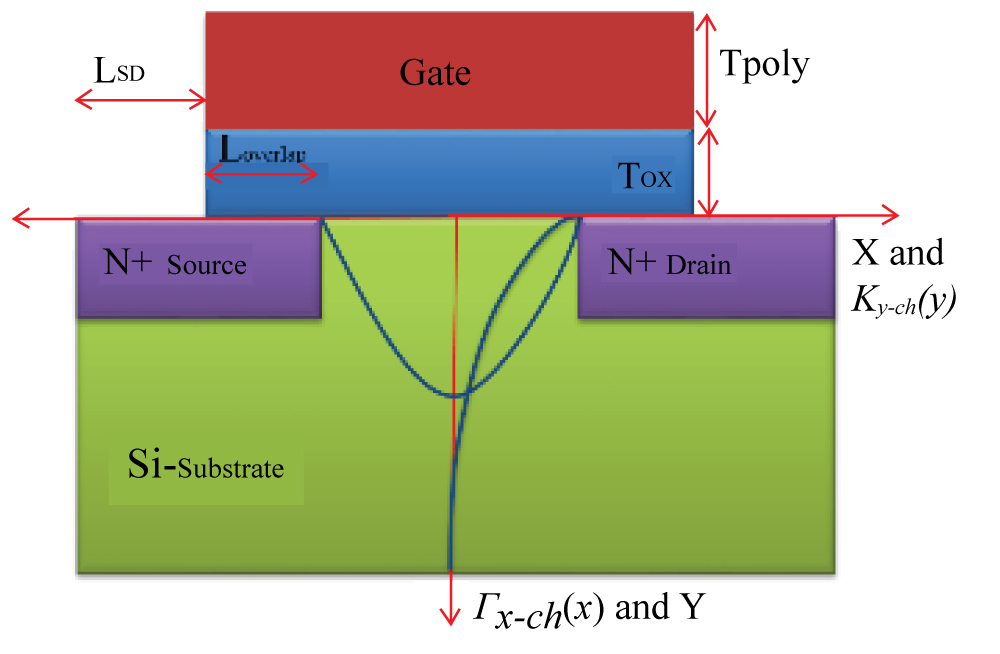
Figure 1: X-direction Gaussian and Y-direction exponentially decreasing doping. Where, Leff = 50 nm, Weff = 1 μm and tox = 1 nm.
X-direction Gaussian and Y-direction exponentially decreasing doping. Where, Leff = 50 nm, Weff = 1 μm and tox = 1 nm.
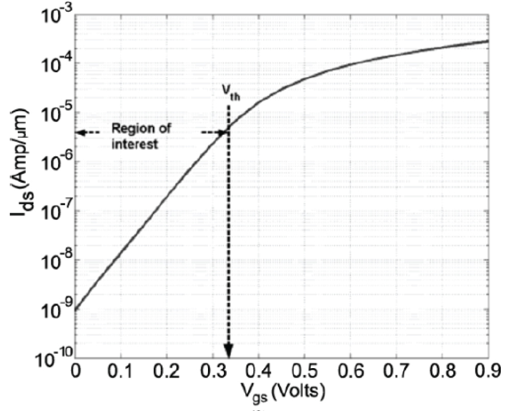
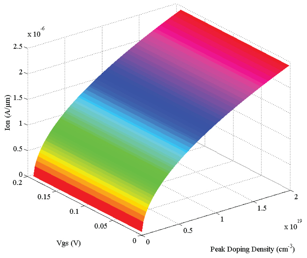
Figure 3: Ion-Vgs-peak doping density for subthreshold device.
Ion-Vgs-peak doping density for subthreshold device.
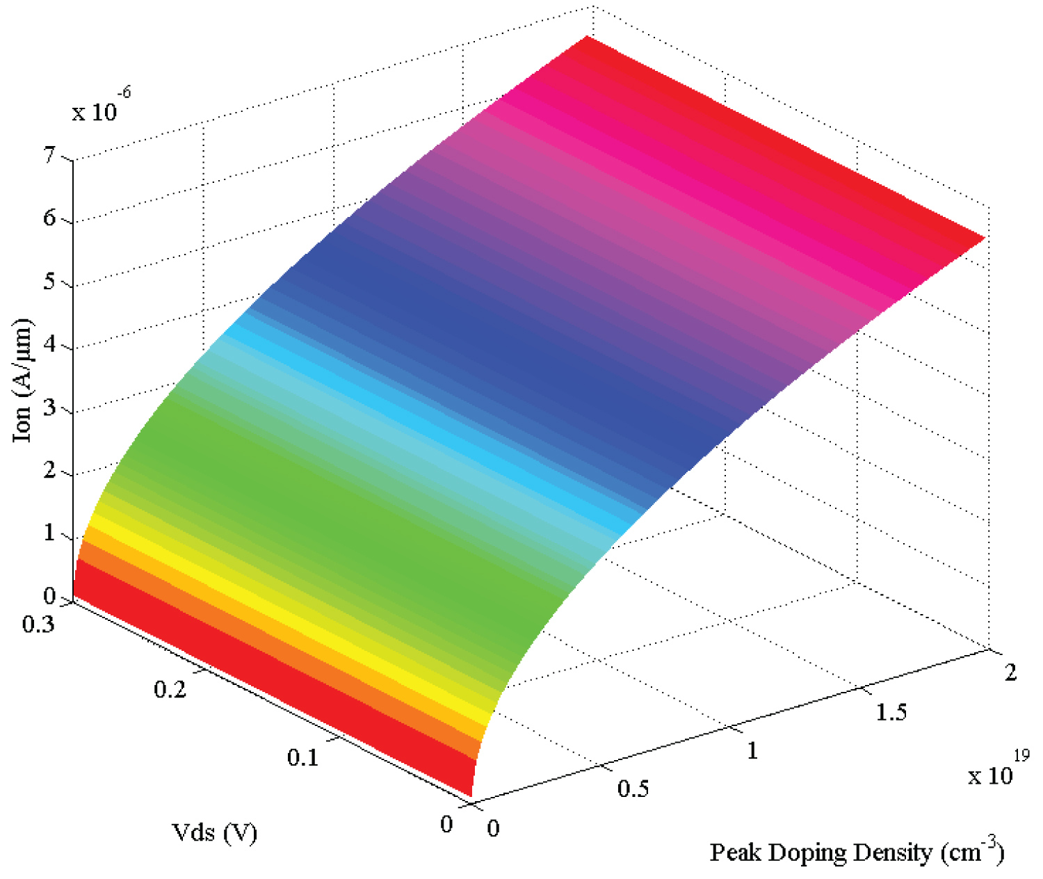
Figure 4: Ion-Vds-peak doping density for subthreshold device.
Ion-Vds-peak doping density for subthreshold device.
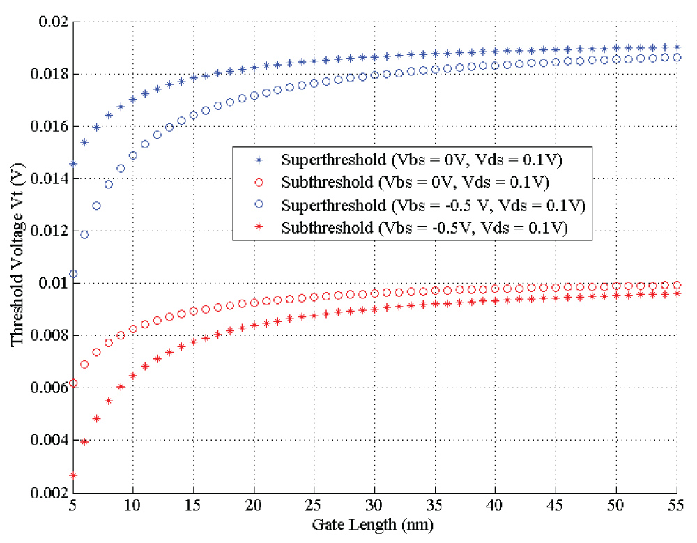
Figure 5: Threshold voltage variation with change of gate length at Vds = 0.1 V and Vbs = 0, -0.5 V. Where...
Threshold voltage variation with change of gate length at Vds = 0.1 V and Vbs = 0, -0.5 V. Where Leff = 50 nm, Weff = 1 μm, doping density at source and drain region NSD = 1.7 × 10¹⁹, tox = 1 nm, T = 300 K.
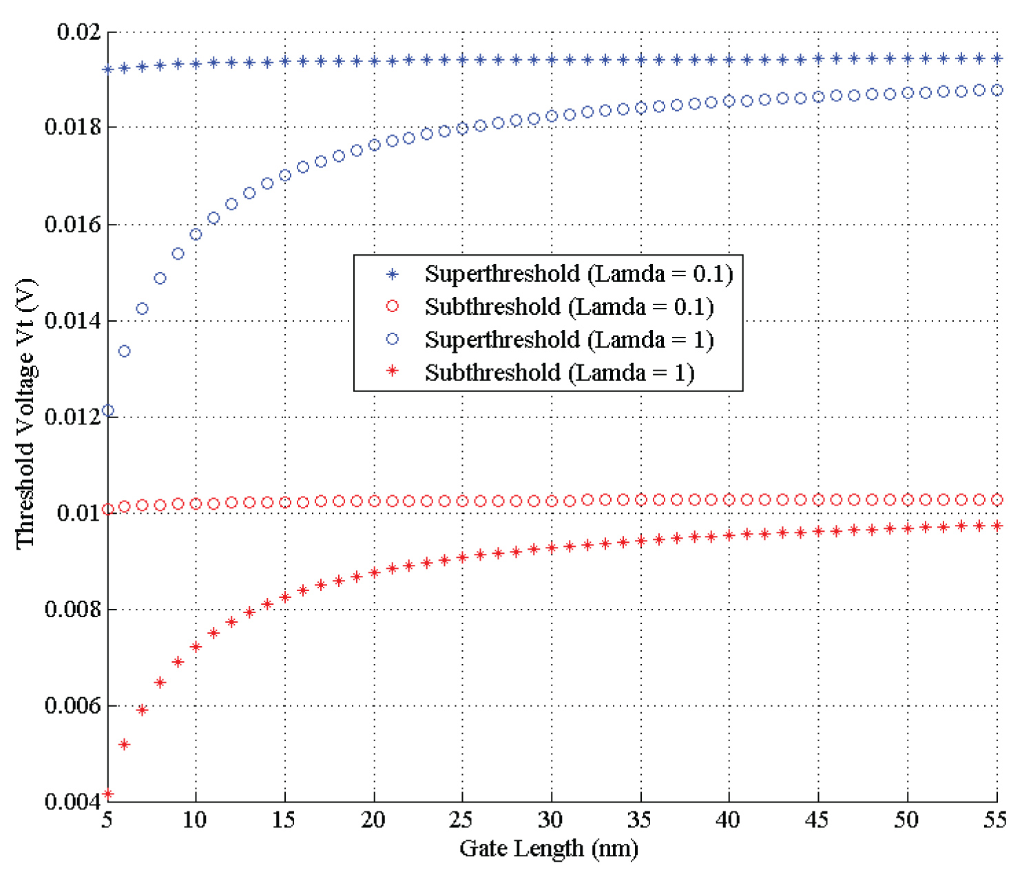
Figure 6: Threshold voltage variation with change of gate length at fitting parameter λ = 0.1 and 1. Where Leff = 50 nm, Weff = 1 μm, ...
Threshold voltage variation with change of gate length at fitting parameter λ = 0.1 and 1. Where Leff = 50 nm, Weff = 1 μm, doping density at source and drain region NSD = 1.7 × 10¹⁹, tox= 1 nm, T = 300 K, Vbs = 0 V, and Vds = 0 .1 V.
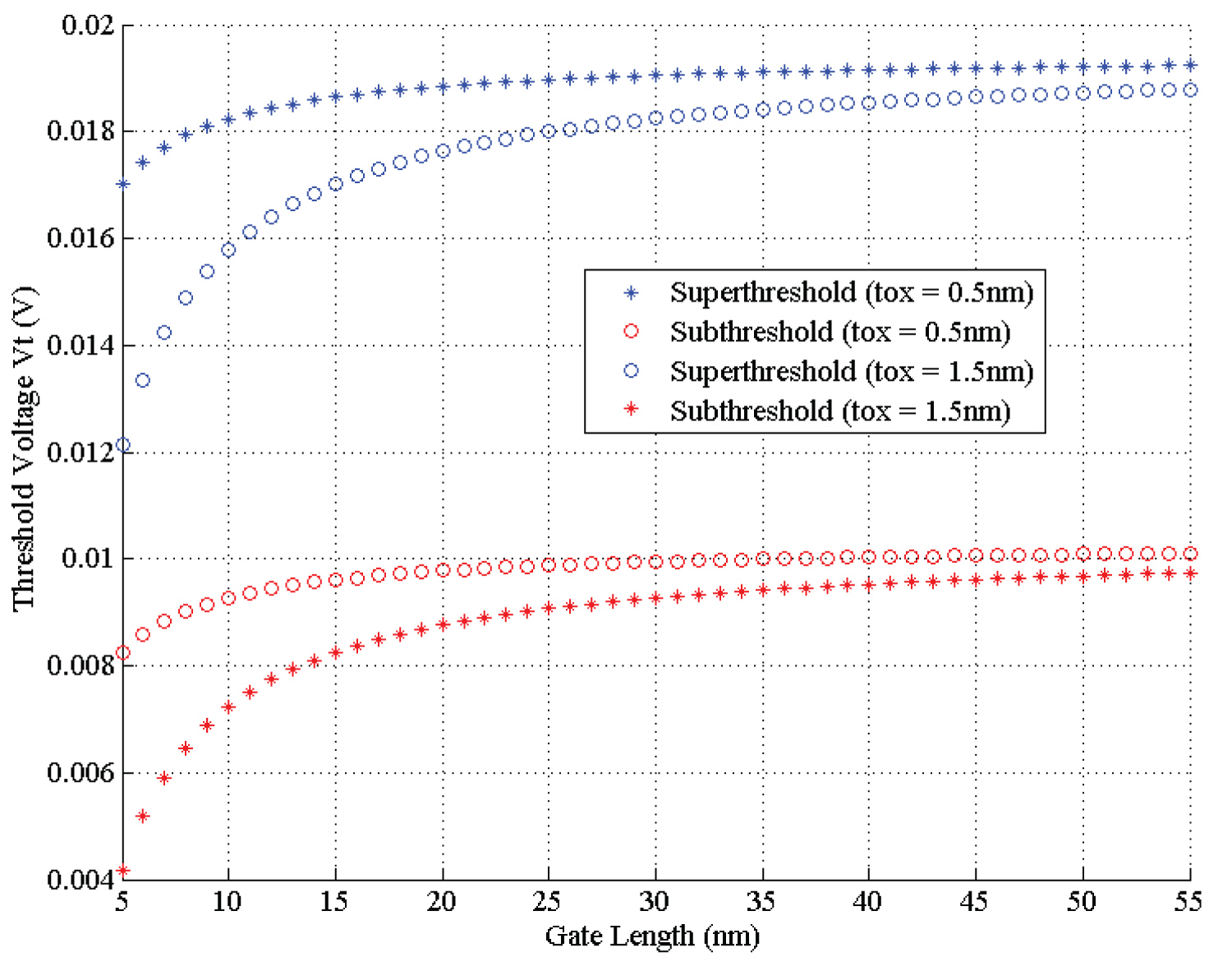
Figure 7: Threshold voltage variation with change of gate length at oxide thickness tox= 0.5 nm and 1.5 nm...
Threshold voltage variation with change of gate length at oxide thickness tox= 0.5 nm and 1.5 nm. Where Leff = 50 nm, Weff = 1 μm, doping density at source and drain region NSD = 1.7 × 10¹⁹ , tox= 1 nm, T = 300 K, Vbs= 0 V, and Vds = 0.1 V.
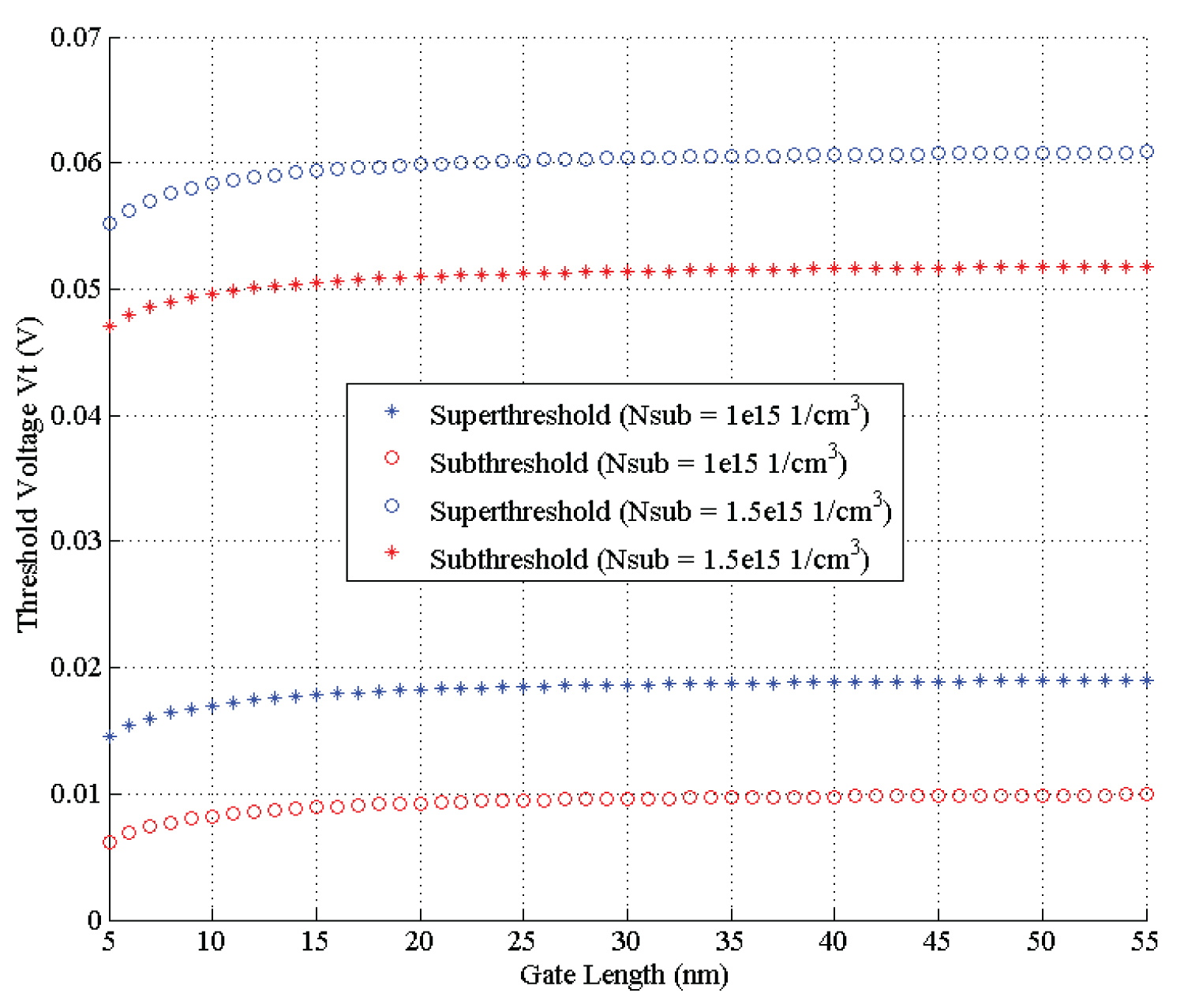
Figure 3: Threshold voltage variation with change of gate length at uniform substrate doping Nsub= 1.0 × 1015 cm-3 and 1.5 × 1015 cm-3...
Threshold voltage variation with change of gate length at uniform substrate doping Nsub= 1.0 × 1015 cm-3 and 1.5 × 1015 cm-3. Where Leff = 50 nm, Weff = 1 μm, doping density at source and drain region NSD = 1.7 × 10¹⁹, tox = 0.5 nm, 1.5 nm, T = 300 K, Vbs = 0 V, and Vds = 0.1 V.
Tables
Table 1: Comparison of Performance Parameters between Subthreshold and Super-Threshold Device.
References
- K Narasimhulu, MP Desai, SG Narendra, VR Rao (2004) The effect of LAC doping on deep submicrometer transistor capacitances and its influence on device RF performance. Electron Devices IEEE Transactions on 51: 1416-1423.
- Hyungsoon Shin, Lee Seungjun (1999) An 0.1-μm asymmetric halo by large-angle-tilt implant (AHLATI) MOSFET for high performance and reliability. Electron Devices IEEE Transactions on 46: 820-822.
- B Cheng, VR Rao, JCS Woo (1999) Exploration of velocity overshoot in a high-performance deep sub-0.1-μm SOI MOSFET with asymmetric channel profile. Electron Device Letters IEEE 20: 538-540.
- BC Paul, A Raychowdhury, K Roy (2005) Device optimization for digital subthreshold logic operation. Electron Devices IEEE Transactions on 52: 237-247.
- Raychowdhury, BC Paul, S Bhunia, K Roy (2005) Computing with subthreshold leakage: Device/circuit/architecture co-design for ultralow-power subthreshold operation. Very Large Scale Integration (VLSI) Systems, IEEE Transactions on 13: 1213-1224.
- ZK Lee, MB McIlrath, DA Antoniadis (1999) Two-dimensional doping profile characterization of MOSFETs by inverse modeling using I-V characteristics in the subthreshold region. Electron Devices IEEE Transactions on 46: 1640-1649.
- Y Taur, TH Ning (1998) Fundamentals of Modern VLSI Devices. Cambridge Univ Press.
- Xing Zhou, Khee Yong Lim, D Lim (2000) A general approach to compact threshold voltage formulation based on 2D numerical simulation and experimental correlation for deep-submicron ULSI technology development [CMOS]. Electron Devices IEEE Transactions on 47: 214-221.
- Liu ZH, C Hu, JH Huang, TY Chan, MC Jeng, et al. (1993) Threshold voltage model for deep-submicrometer MOSFETs. Electron Devices IEEE Transactions on 40: 86-95.
- Godoy A, JA López Villanueva, JA Jiménez Tejada, A Palma, F Gámiz (2001) A simple subthreshold swing model for short channel MOSFETs. Solid-State Electronics 45: 391-397.
- Munem Hossain, Masud H Chowdhury (2016) Comprehensive doping scheme for MOSFETs in ultra-low-power subthreshold circuits design. Microelectronics Journal 52: 73-79.
Author Details
Munem Hossain* and Masud H Chowdhury
Computer Science and Electrical Engineering, University of Missouri, USA
Corresponding author
Munem Hossain, Computer Science and Electrical Engineering, University of Missouri, Kansas City, MO 64110, USA, Tel: 1-816-235-2432, Fax: 1-816-235-5159.
Accepted: March 13, 2018 | Published Online: March 15, 2018
Citation: Hossain M, Chowdhury MH (2018) Modified Ion Implantation Based New Subthreshold Device Design & Threshold Voltage Modelling for Ultra Low Power Applications. Int J Electron Device Phys 2:003.
Copyright: © 2018 Hossain M, et al. This is an open-access article distributed under the terms of the Creative Commons Attribution License, which permits unrestricted use, distribution, and reproduction in any medium, provided the original author and source are credited.
Abstract
This paper introduces threshold voltage modelling of new doping profile for devices to be used in subthreshold circuit applications. The proposed scheme addresses doping variations along all dimensions of device. This new doping scheme proposes to employ Gaussian distribution of doping concentration along length of the channel with highest concentration at middle of channel. Doping concentration across the depth of the device is exponentially decreasing with channel surface at the highest concentration. Results show that the optimized device with the proposed doping profile offers higher Ion current in the subthreshold device. In this paper threshold voltage modelling has been done and comparison made between superthreshold and subthreshold device threshold voltage. Threshold voltage comparison result shows that proposed subthreshold device operates at lower threshold voltage and less threshold variation in compare to existing devices.
Keywords
Biochip, Subthreshold and superthreshold operation, Ultra-low-power circuit, Doping profile, Halo & retrograde profile.
Introduction
Proper ion implantation or Doping is one of the most critical design decisions for deeply scaled CMOS devices. For emerging system-on-chip (SOC) applications doping is very challenging due to the conflicting requirements of the analog and digital circuits. It is observed that with lateral asymmetric channel (LAC) doping the total gate capacitance of a transistor is reduced by almost 10% in the saturation region at 100 nm technology node compared to the conventional MOSFETS [1,2]. Transistor capacitances have significant influences on its RF performance. In [3], it is demonstrated that the electron velocity in the inversion layer of a novel thin film silicon-on-insulator (SOI) device is affected by doing profile.
In conventional integrated circuits, short-channel devices are usually optimized for operation in superthreshold region to ensure higher mobility, lower drain-induced barrier lowering (DIBL), reduced leakage, and minimal threshold voltage roll-off. However, a transistor optimized for superthreshold circuit may not be optimal for the subthreshold region where effects like DIBL, threshold voltage roll-off and electron/hole tunneling are much less significant [4]. As a consequence, high doping traditionally used in superthreshold device to overcome the short-channel effect (SCE) will not be critical for subthreshold operation [5]. In superthreshold device, the main functions of halo and retrograde dopings are to reduce DIBL, prevent body punch through and control the threshold voltage of the device independent of its subthreshold slope. Since DIBL, body punch through and threshold voltage variation are not severe in subthreshold device due to lower supply voltage, the halo and retrograde doping is not required for such design. High to low doping profile [4] has been proposed for subthreshold operation.
An attempt has been made to explore a set of new doping profiles for devices to be used in subthreshold circuit. It has been outlined the general principle of this new doping scheme. In this paper, we have presented one of them for the devices in subthreshold circuits (Figure 1). The rest of the paper is organized as follows. Section II illustrates the concept of our new doping scheme under our investigation. Section III presents the mathematical models and the analysis of the new doping profile. Section IV presents the threshold voltage mathematical modelling and comparison between superthreshold and subthreshold device. Finally, Section V concludes the paper with a brief discussion of our ongoing and future work.
Proposed Doping Scheme for Subthreshold Device
The proposed doing scheme would bring changes in doping properties along the length (X direction) and depth (Y direction) of the device and keep the doping concentration along the width constant. The doping profile in X direction is kept somewhat constant in most of the previous designs and only the Y direction doping profiles have been varied. We propose a three-dimensional doping scheme, where doping profiles would be varied in both directions. We propose to adopt Gaussian distribution of doping density in the X direction and we are exploring four different doping profiles in the Y directions for subthreshold devices. Based on the proposal we would get four possible combinations of two-dimensional doping profiles. The focus of this paper is to illustrate the doping profile presented in Figure 2. In this project, we plan to show that lower threshold voltage can be achieved in the subthreshold device by redesigning the devices compare to superthreshold device.
In the rest of this section we have analyzed the performance of the proposed doping profiles for the subthreshold device compared to a superthreshold device. In Figure 1, threshold voltage Vth ~0.3 V under which the device is considered OFF. On the other hand the operating region of a subthreshold device is completely moved to the subthreshold region (0 V to 0.3 V in Figure 1). Within that subthreshold region the subthreshold device must have distinguishable OFF and ON states. Therefore, our area of interest in Figure 1 is the subthreshold region, where a voltage very close to 0 V will be considered as the OFF state and a voltage close to Vth would be considered as the ON state. In all the simulations below we define a device as a superthreshold device if it uses the conventional halo and retrograde doping profile and it is optimized for the operation in the linear and saturation regions (above Vth ~ 0.3 V) of a MOSFET.
Mathematical Modelling and Analysis of the Proposed New Three Dimensional Doping Profiles
A technique based on the subthreshold current-voltage (I-V) characteristics to extract 2-D doping profiles is proposed in [6]. Here we propose a new doping profile for subthreshold device operation using similar approach. We modeled MOSFET subthreshold current based on the proposed doping profile. The formulation of the model is shown for NMOS transistor and can be easily applied to PMOS transistor. The 2D Gaussian doping profile in the channel can be represented as in (1) [6].
Equations (2) and (3) represents X dimension doping distribution for subthreshold and superthreshold device operation. Here (4) illustrates the exponentially decreasing Y dimension (from the channel surface towards the body) doping profile for the subthreshold device.
Here d is the depth of the device (measured from the channel surface to the bottom surface of the substrate). The parameter αch controls the position and σ1y-ch controls the variance of exponentially decreasing doping profile along Y-direction. Here αch = 0 means that the variation of doping concentration starts from the surface of the channel and the parameters have chosen for σ1y-ch = 21 nm, σ1x-ch = 10 nm.
In subthreshold operation the bias voltage is less than that of superthreshold operation. Therefore, the doping profile for subthreshold operation has to be optimized for low bias voltage. The subthreshold current flowing through the transistor can be given by (5) [7]. The Isub model used in this study is suitable for deep sub micrometer MOSFET. In reference [4] for high to low doping profile and 40-60 nm subthreshold devices design this Isub model is used for their simulation. In our 50 nm node we have used this Isub model.
In (5), Ncheff is the effective channel doping, Φs is the surface potential, m is the body effect and VT is the thermal voltage. Different parameters in the above model depend on the effective channel doping. The effective channel doping can be calculated by (6), where Δch is the area of the channel region that under the influence of the gate. The X and Y directional doping profiles in (6) would be calculated using (2), (3) and (4).
The 3-D plot in Figure 3 and Figure 4 shows the combined changes of Ion with the variations of gate and drain bias voltage and the peak doping density. Based on the 3-D plot, the optimum value of Ion can be found for a specific set of peak doping density and Vgs, Vds values. Furthermore, Random dopant fluctuation is also an important factor for device performance which depends on the vertical and horizontal electric field of the channel. Since the gate voltage and biasing voltage is very small the impact of both electric fields will not be strong enough to cause random dopant fluctuation in the channel area.
Threshold Voltage Modelling of the New Doping Profile
In subthreshold operation the current flowing from the drain to source of the transistor is known as the subthreshold current. In (7), Vbi is the source/drain built-in potential and Nsd is the doping concentration in the lightly doped region.
In (8) and (9), Φs0 is the surface potential and Φ01 is the short-channel surface potential. It is found that potential-barrier lowering is needed in addition to the charge-sharing effect since they describe different contributions to the observed SCE (Vt roll-off) [8].
From the quasi 2D model [9] the surface potential ΦS in short channel device is lowered by ΔΦS due to source/drain finger fields. And it is smaller than 2ΦB (bulk potential) at strong inversion condition. In (11), ΔΦS is the function of the characteristics length lα and α is the fitting parameter.
Using charge sharing model the threshold voltage [8,10] can be expressed as in (13).
Here VFB is the flat band voltage, Φs0 is the zero bias surface potential, γ is the body factor, Xd is the depletion layer thickness, and λ is a fitting parameter (~1) [8,10,11]. Φs of short channel devices from its zero bias value due to short channel effect like DIBL and Vth roll off.
Figure 5 shows how threshold voltage is varying with the change of gate length. Super threshold device shows higher threshold voltage as compared to the subthreshold device. Also comparison has been made for different body biases (Vbs = 0, -0.5 V) for different types of device. Negative body bias improves the threshold voltage for both superthreshold and subthreshold device operation. In both cases, Vds is kept constant to make fair comparison. Proposed doping profile for the subthreshold device improves the threshold voltage, which will lead the device to go to ON state even faster. Figure 6 shows the impact of the fitting parameter λ on the threshold voltage. At λ = 0.1 the threshold voltage is constant with the variation of the gate length, but for λ= 1 the threshold voltage significantly varies with the variation of the gate length. Higher λ reduces the threshold voltage in both the cases of superthreshold and subthreshold devices. Figure 7 shows the impact of oxide thickness on the threshold voltage variation. Under proposed doping profile and constant oxide thickness subthreshold device has lower threshold voltage than the super threshold device. Channel length below 25 nm has more impact on threshold voltage for specific oxide thickness. Figure 8 shows the impact of uniform substrate doping on the threshold voltage. Higher substrate doping increases the threshold voltage for both superthreshold and subthreshold devices. Therefore, uniform substrate doping profile is one of the important performance parameters for tuning the desired threshold voltage for low power subthreshold circuit design.
In our work, we basically showed, if the existing device is operating below threshold (which is Super-Threshold Device here in Table 1) voltage then performance parameter will degrade. We have proposed a new doping profile for the subthreshold device that showed better performance parameters compared to other. In the comparison below we have seen higher leakage current but this is because we are operating our device comparatively at the lower threshold voltage. However, all the performance parameter listed in Table 1 shows better performance compared to the superthreshold device.
Conclusion and Future Work
This paper presents a study of the doping profile optimization in the channel for subthreshold operation. In 3D plot we have shown the controlled variation of Ion with VFrom the quasi 2D model, Vgs and peak doping density for subthreshold device with this new doping profile. We have also modeled the threshold voltage for new doping profile and shown the threshold voltage variation with different device parameters. Our threshold voltage comparison result shows that subthreshold device operate at lower threshold voltage in compare to superthreshold device. By choosing optimum Substrate doping, oxide thickness, lamda and body bias the subthreshold device threshold voltage variation can be controlled precisely. We have described the concept of different doping scheme with other basic performance parameters. Our future work will cover all other options under our investigation and address all the factors of this new subthreshold device.